Researchers have developed a new method to display highly realistic holographic images using “holobricks,” which can be stacked together to create large-scale holograms. Photo credit: University of Cambridge Researchers have developed a new method to display highly realistic holographic images using “holobricks,” which can be stacked together to create large-scale holograms. Researchers from the University of Cambridge and Disney Research developed a holobrick proof-of-concept that can stitch holograms into one large seamless 3D image. This is the first time this technology has been demonstrated and opens the door to scalable 3D holographic displays. The results are published in the journal Light: Science & Applications. As technology evolves, people want high-quality visual experiences, from high definition 2D television to 3D holographic augmented or virtual reality and large true 3D displays. These displays must support a significant flow of data: for a 2D Full HD display, the information data rate is about three gigabits per second (Gb/s), but a 3D display with the same resolution would require a rate of three terabit per second, the is not yet available. Holographic displays can reconstruct high quality images for a true 3D visual experience. They are considered the ultimate display technology to connect the real and virtual worlds for immersive experiences. Reconstructed holographic images of a toy train using holobricks (top) and original image captured by a camera (bottom). Photo credit: University of Cambridge “Providing an adequate 3D experience with current technology is a major challenge,” said Professor Daping Chu from the Department of Engineering in Cambridge, who led the research. “Over the past decade, we have been working with our industry partners to develop holographic displays that enable the simultaneous realization of large dimensions and large fields of view, which must be matched with a hologram with a large optical information content.” However, the information content of current hologram information is much greater than the display capabilities of current light engines known as spatial light modulators due to their limited spatial bandwidth product. With 2D displays, it is common to tile small displays to form a large display. The approach examined here is similar, but for 3D displays, which has not been done before. “Stitching pieces of 3D images together is non-trivial because the final image needs to be seen as seamless from all angles and all depths,” said Chu, who is also director of the Center for Advanced Photonics and Electronics (CAPE). “Direct tiling of 3D images in real space is just not possible.” To address this challenge, researchers developed the holobrick unit, which relies on coarsely integrated holographic displays for angularly tiled 3D images, a concept developed at CAPE with Disney Research about seven years ago. Each of the holobricks uses a high information bandwidth spatial light modulator to convey information in conjunction with coarse-grain integrated optics to form angularly tiled 3D holograms with large viewing areas and fields of view. Careful optical design ensures that the holographic stripe pattern fills the entire surface of the holobrick, allowing multiple holobricks to be seamlessly stacked to form a scalable, spatially tiled 3D holographic display that offers both a wide viewing angle and large size . The proof-of-concept developed by the researchers consists of two seamlessly tiled holobricks. Each full-color brick is 1024 × 768 pixels with a 40° field of view and 24 frames per second to display tiled holograms for full 3D images. “There are still many challenges to make ultra-large 3D displays with wide viewing angles, such as Like a 3D holographic wall,” Chu said. “We hope that this work can offer a promising avenue to solve this problem, based on the currently limited display capabilities of spatial light modulators.” Reference: “Holobricks: Modular Grob Integral Holographic Displays” by Jin Li, Quinn Smithwick and Daping Chu, March 16, 2022 Light: Science & Applications.DOI: 10.1038/s41377-022-00742-7

How to clean Holi colour stains from your smartphone, other electronic devices
Holi is just around the corner. While we’re all busy getting ready for the Holi party – food, colors, music – it’s also important that we prepare to keep all our electronic devices, including our smartwatches, earbuds and smartwatches, safe during Holi. So here are a few tips and tricks that will help you keep your electronic devices safe during Holi. And in case you manage to get holi color stains on it, we have listed a number of tricks to help you clean your devices afterwards. Also Read – Call of Duty Mobile Announces New Free Holi Rewards: How to Claim Them How to protect your smartphone and other devices while playing Holi – One of the many ways you can keep all your gadgets stain and water free is by placing them in a ziplock bag or plastic backing. You can still carry your essentials like your earbuds and smartphone, but adding a layer of cover keeps them clean and dry. Also Read – Holi Sale Offers: Vivo Announce Cashback Offers of up to Rs 3,500 on Vivo V23 Series – You can also try to cover all ports and openings of your electronic devices with tape. This prevents the paints and even water from reaching the hard-to-clean areas of your equipment. Also Read: Facebook Adds Holi Stickers for Users in India. Here’s how you can use them – Use a screen protector and a silicone case to keep smartphones safe. These also protect it from accidental drops. How to clean your smartphone and other electronic devices after Holi – One of the easiest ways to clean your smartphone and other electronics like earphones and smartwatch after the Holi party is to dab a soft tissue or cotton pads in liquid hand sanitizer and gently rub the color markers on your phone. – For stubborn paint stains that won’t go away, try rubbing alcohol instead. – Use masking tape to remove colored connectors and vents from your devices. Supplement it with liquid alcohol and a handkerchief. This will completely clean all ports and openings. – When cleaning your smartwatch, you can use rubbing alcohol and a soft cloth to clean the face and nylon strap, and a clean cloth to remove paint from the metal strap. – In case you drop your phone in water, keep it in a bowl of uncooked rice. Change its position periodically to allow all liquid to drain from the device. Don’t turn it on, it may cause short circuit, and don’t use hair dryer directly.

How to collaborate, draft emails in Google Doc and export them to Gmail
Google Docs is getting a new draft email template after the last update. The new feature in Google Docs makes it easier to collaborate on a draft email. It allows users to draft emails via Google Doc draft template and then export them to Gmail. Also read – McLaren F1 cars get Google Chrome-style wheels this year, Android bot The tech brand introduced it as part of the smart canvas push that brought the “@menu” to Google Docs, allowing users to easily paste data and details from other Google services. As for the new feature, Google Doc users can now collaborate with other team members when composing an email. The email draft template can be accessed by typing @email in a Google Doc, which will show a template with To, Cc, Bcc, and Subject. Once the email is ready to be sent, you can simply click on the Gmail icon on the left. How to start – Also read – Google announces the dates of IO 2022 with an interactive puzzle How to collaborate with team members in Google Docs and send an email – To insert an email template first, go to Insert > Building Blocks > Email Draft Also read – Google will soon let you pay for parking with your voice: Here’s how – To collaborate with team members on an email, visit docs.google.com in any web browser -Then click the “+” icon to create a new document or use an existing one – Next, type ‘@email’ in a google doc -Once you’re ready to send the email, just select the Gmail icon to export your draft to the email service, and the Gmail compose window will appear and all the email fields will automatically populate with it be filled out with the details you entered Draft email in Doc. The Google Docs email draft template, originally unveiled in February, is now being made available to all Google Workspace, G Suite Basic, and Business customers.
Building a Heart One Layer at a Time Using Advanced 3D Bioprinting Techniques
Mark Skylar-Scott and his team of Stanford bioengineers aim to use advanced 3D printing techniques to turn a paste of living cells into hearts and other organs. Few human organs are more alluring to an engineer than the human heart. Its chambers pump in perfect unison; its materials are pliable but contract when needed; Its shape and movement are perfectly tuned to efficiently push fluid throughout the body. It’s a structural marvel – but when something goes wrong within this structure, the inherent complexity makes it a real challenge to fix it. Thousands of young patients with congenital heart defects therefore have to cope with their disease for the rest of their lives. “Pediatric heart disease is one of the most common forms of congenital birth defects in the United States,” said Mark Skylar-Scott, assistant professor of bioengineering in the engineering and medical schools. “It’s really hard for families. There are ways to extend children’s lives through surgery, but many children suffer from restricted mobility and live uncertain lives. To find a truly healing solution, you must somehow replace damaged or malformed tissue.” Stanford scientists are working to make human tissue on a therapeutic scale, with a focus on the heart. Photo credit: Kurt Hickman That’s where Skylar-Scott comes in. He is working on new ways to tackle congenital heart defects by creating artificial heart tissue in the lab. It takes far more than just culturing cells in a dish, he notes. Most existing techniques deploy heart cells or stem cells on a temporary “scaffold”: a porous, spongy substance that can hold them in place in three dimensions. Although this method allows researchers to grow lab-made tissue, it is only really practical for extremely thin layers of cells. “If you have a scaffold that’s only a few cells thick, you can put the cells in the right place. But when you try to grow something that’s an inch thick, it becomes really difficult to seed cells in the right places to grow tissue. Keeping them alive, giving them the right nutrients, or vascularizing them becomes a real challenge,” says Skylar-Scott. Human organs are also not monolithic clumps of cells, he adds. Each is made up of complex layers of multiple cell types, resulting in a 3D structure that is incredibly difficult to replicate. Print organoids To circumvent this fact, Skylar-Scott and his team are working on a bold new approach to organ engineering. Using advanced 3D printing techniques, they craft thick tissues layer by layer, placing exactly the kind of cells needed in the right places, like a tower rising from a lattice of carefully placed bricks. This type of construction method, he notes, lends itself well to replicating complex tissues like the heart, where 3D shape is critical to its function. As promising as it may be, cellular 3D printing comes with some profound and thorny challenges. Unlike plastic filaments, which consumer 3D printers can heat and press into myriad shapes, cells are alive. They’re soft, squishy, imperfect, and frustratingly fragile, says Skylar-Scott. The 3D bioprinter prints a pattern. Credit: Andrew Brodhead “If you try to place a single cell at a time, printing a liver or a heart can take hundreds or thousands of years. Even if you’re processing 1,000 cells per second, you still have to lay down many billions of cells to get an organ. If you do the math, it doesn’t look so good for a scalable process,” he says. Instead, Skylar-Scott and his lab are working to speed up the printing process by depositing dense clumps of cells called “organoids.” The group makes these clumps by putting genetically engineered stem cells in a centrifuge, which creates a pasty substance. With this concoction, they can print large numbers of cells at once into a gelatinous 3D structure. “We basically define the large-scale structure of an organ by printing these organoids,” he says. cell programming However, attaching the stem cells is only the first step. Once printed, researchers must somehow convince them to differentiate into more specific cell types and form a multi-layered cluster of functioning groups of cells that resemble healthy organ tissue. To achieve this, Skylar-Scott essentially bathes the stem cells in a chemical cocktail. “Each line of stem cells that we develop is genetically engineered to respond to a specific drug,” he notes. “Once they sense this drug, they differentiate into specific cell types.” Some cells are programmed to become cardiomyocytes, the heart cells that make up the functional core tissue in the heart. Others are instructed to become stromal cells that connect tissues together. Skylar-Scott tests his printed tissues in a bioreactor, a smartphone-sized container that helps keep the printed cells alive. Inside, his team managed to grow a printed organ-like structure: a tube about 2 inches long and half a centimeter in diameter. Like a vein in the human body, this tiny device could “pump” itself, contracting and expanding to move fluid through itself. “If we can engineer more tissues like this, we might have a good halfway to building something that can be implanted in the human body,” says Skylar-Scott. “In patients who were born with a single ventricle, for example, there is only one chamber in the heart that can push blood to the body and lungs – which puts a lot of strain on the cardiovascular system and leads to high blood pressure, which organs produce can harm. Something like this could act as a biological pumping device to move blood to and from the heart,” he says. Enlarge Skylar-Scott quickly realizes that the printing of a larger structure, such as a functional chamber, grafted onto an existing heart is a long way off. To accomplish that would mean growing a little more than 16 times the size of his lab’s experimental “vein pump.” To make anything even close to that size — or better yet, a whole new organ — his lab would have to increase cell production tremendously. “Scale-up will be the challenge of our
New Algorithm Helps Quantum Computer Crunch Chemistry Equations
The hybrid algorithm uses a classical and a quantum computer to calculate the ground-state energy. This will help researchers develop new materials for various applications, including sustainability goals. Credit: Nicoletta Barolini Quantum computers are getting bigger, but there are still few practical ways to harness their extra processing power. To overcome this hurdle, researchers are designing algorithms that should facilitate the transition from classical to quantum computers. In a new study in Nature, Researchers unveil an algorithm that reduces the statistical errors, or noise, generated by quantum bits, or qubits, in crunchy chemical equations. The algorithm, developed by Columbia chemistry professor David Reichman, and postdoc Joonho Lee with Google Quantum AI researchers, uses up to 16 qubits on Sycamore, Google’s 53-qubit computer, to calculate the ground-state energy that lowest energy state of a molecule. “These are the largest quantum chemical calculations ever performed on a real quantum device,” Reichman said. The ability to accurately calculate the ground-state energy will enable chemists to design new materials, said Lee, who is also a visiting researcher at Google Quantum AI. The algorithm could be used to design materials to accelerate nitrogen fixation for agriculture and hydrolysis to generate clean energy, among other sustainability goals, he said. The algorithm uses a quantum Monte Carlo, a system of methods for calculating probabilities when a large number of random, unknown variables are involved, as in a roulette game. Here, the researchers used their algorithm to determine the ground-state energy of three molecules: heliocide (H4), using eight qubits for the calculation; molecular nitrogen (N2) with 12 qubits; and Solid Diamond with 16 qubits. Ground-state energy is affected by variables such as the number of electrons in a molecule, the direction in which they spin, and the orbits they take when orbiting a nucleus. This electronic energy is encoded in the Schrödinger equation. Solving the equation on a classical computer becomes exponentially more difficult as the molecules get larger, although methods of estimating the solution have made the process easier. How quantum computers could circumvent the exponential scaling problem has been an open question in this area. In principle, quantum computers should be able to perform exponentially larger and more complex calculations, such as those required to solve the Schrödinger equation, because the qubits that make them up use quantum states. Unlike binary digits, or bits, which are made up of ones and zeros, qubits can exist in two states at the same time. However, qubits are vulnerable and error-prone: the more qubits used, the less accurate the final answer will be. Lee’s algorithm uses the combined power of classical and quantum computers to solve chemical equations more efficiently while minimizing quantum computer errors. “It’s the best of both worlds,” Lee said. “We used tools that we already had and tools that are considered state-of-the-art in quantum information science to refine quantum computational chemistry.” A classical computer can handle most of Lee’s quantum Monte Carlo simulations. Sycamore jumps in for the last, most computationally complex, step: calculating the overlap between a trial wave function — an estimate of the mathematical description of the ground-state energy that can be implemented by the quantum computer — and a sample wave function, which is part of the Monte Carlo statistical process. This overlap provides a set of constraints, called boundary conditions, on the Monte Carlo samples that ensure the statistical efficiency of the computation (see Lee’s webinar for more details on the math). The previous record for solving the ground-state energy used 12 qubits and a method called the Variational Quantum Eigensolver, or VQE. But VQE ignored the effects of interacting electrons, an important variable in the calculation of the ground-state energy that Lee’s quantum Monte Carlo algorithm now includes. Adding virtual correlation techniques from classical computers could help chemists tackle even larger molecules, Lee said. The hybrid classical quantum calculations in this new work turned out to be as accurate as some of the best classical methods. This indicates that problems could be solved more accurately and/or faster with a quantum computer than without – an important milestone for[{” attribute=””>quantum computing. Lee and his colleagues will continue to tweak their algorithm to make it more efficient, while engineers work to build better quantum hardware. “The feasibility of solving larger and more challenging chemical problems will only increase with time,” Lee said. “This gives us hope that quantum technologies that are being developed will be practically useful.” Reference: “Unbiasing Fermionic Quantum Monte Carlo with a Quantum Computer” 16 March 2022, Nature.DOI: 10.1038/s41586-021-04351-z

Molecular Engineers Show How To Make “Computer” Out of Liquid Crystals
Researchers from the University of Chicago’s Pritzker School of Molecular Engineering set out how liquid crystals could be used to perform calculations using techniques like the one pictured above, where the redder region is activated by light. Photo Credit: Image courtesy of Rui Zhang The UChicago breakthrough could pave the way for applications in robotics, computers using soft materials. researchers with the[{” attribute=””>University of Chicago Pritzker School of Molecular Engineering have shown for the first time how to design the basic elements needed for logic operations using a kind of material called a liquid crystal—paving the way for a completely novel way of performing computations. The results, published recently in Science Advances, are not likely to become transistors or computers right away, but the technique could point the way towards devices with new functions in sensing, computing and robotics. “We showed you can create the elementary building blocks of a circuit—gates, amplifiers, and conductors—which means you should be able to assemble them into arrangements capable of performing more complex operations,” said Juan de Pablo, the Liew Family Professor in Molecular Engineering and senior scientist at Argonne National Laboratory, and the senior corresponding author on the paper. “It’s a really exciting step for the field of active materials.” The details in the defects The research aimed to take a closer look at a type of material called a liquid crystal. The molecules in a liquid crystal tend to be elongated, and when packed together they adopt a structure that has some order, like the straight rows of atoms in a diamond crystal—but instead of being stuck in place as in a solid, this structure can also shift around as a liquid does. Scientists are always looking for these kinds of oddities because they can utilize these unusual properties as the basis of new technologies; liquid crystals, for example, are in the LCD TV you may already have in your home or in the screen of your laptop. One consequence of this odd molecular order is that there are spots in all liquid crystals where the ordered regions bump up against each other and their orientations don’t quite match, creating what scientists call “topological defects.” These spots move around as the liquid crystal moves. Scientists are intrigued by these defects, wondering if they could be used to carry information – similar to the functions that electrons serve in the circuits of your laptop or phone. But in order to make technology out of these defects, you’d need to be able to shepherd them around where you want them, and it’s proved very difficult to control their behavior. “Normally, if you look through a microscope at an experiment with an active liquid crystal, you would see complete chaos—defects shifting around all over the place,” said de Pablo. But last year, an effort from de Pablo’s lab headed by Rui Zhang, then a postdoctoral scholar at the Pritzker School of Molecular Engineering, in collaboration with Prof. Margaret Gardel’s lab from UChicago and Prof. Zev Bryant’s lab from Stanford, figured out a set of techniques to control these topological defects. They showed that if they controlled where they put energy into the liquid crystal by shining a light only on specific areas, they could guide the defects to move in specific directions. In a new paper, they took it a logical step further and determined that it should be theoretically possible to use these techniques to make a liquid crystal perform operations like a computer. “These have many of the characteristics of electrons in a circuit—we can move them long distances, amplify them, and shut or open their transport as in a transistor gate, which means we could use them for relatively sophisticated operations,” said Zhang, now an assistant professor at the Hong Kong University of Science and Technology. Though calculations suggest these systems could be used for computations, they are more likely to be uniquely useful in applications such as the field of soft robotics, the scientists said. Researchers are interested in soft robots—robots with bodies that aren’t made out of hard metal or plastic, but rather stretchy and soft materials—because their flexibility and gentle touch means they can perform functions that hard-bodied robots cannot. The team can imagine creating such robots that can do some of their own “thinking” using active liquid crystals. “It’s not often that you are able to see a new way to do computing.” — Prof. Juan De Pablo They can also imagine using topological defects to ferry small amounts of liquid or other materials from place to place inside tiny devices. “For example, perhaps one could perform functions inside a synthetic cell,” said Zhang. It’s possible that nature already uses similar mechanisms to transmit information or perform behaviors inside cells, he said. The research team, which also includes co-author and UChicago postdoctoral researcher Ali Mozaffari, is working with collaborators to carry out experiments to confirm the theoretical findings. “It’s not often that you are able to see a new way to do computing,” de Pablo said. Reference: “Logic operations with active topological defects” by Rui Zhang, Ali Mozaffari and Juan J. de Pablo, 23 February 2022, Science Advances.DOI: 10.1126/sciadv.abg9060 This work used resources of the University of Chicago Materials Research Science and Engineering Center. Funding: National Science Foundation, Hong Kong Research Grants Council.
Groundbreaking X-Ray Lens Provides Incredible Glimpse Into the Nanoworld
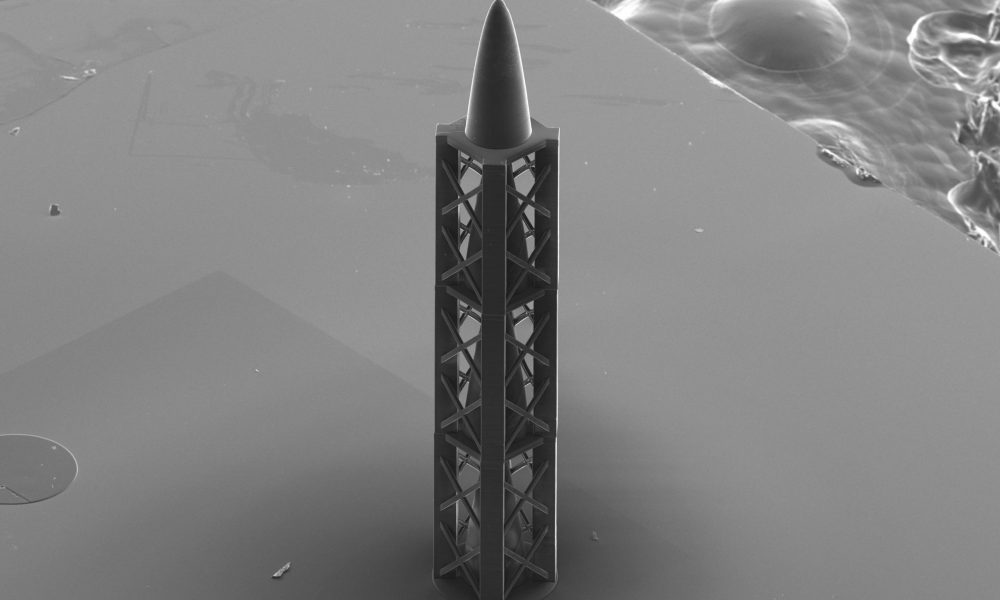
A microstructure from the 3D printer: almost a millimeter long (or high, as in the photo) is the new refractive structure that was developed by PSI scientists and, in combination with a diffractive element, results in an achromatic X-ray lens. Turned on its end, it resembles a miniature rocket. It was made from a special type of polymer by a 3D printer. This picture of the structure was taken with a scanning electron microscope. Photo credits: Paul Scherrer Institute/Umut Sanli Scientists at the Paul Scherrer Institute have developed a pioneering achromatic lens for X-rays. This means that the X-rays can be precisely focused onto a single point, even if they have different wavelengths. The new lens will greatly facilitate the study of nanostructures with X-rays, according to an article the researchers just published in the journal nature communication. Achromatic lenses are essential for producing sharp images in photography and in optical microscopes. They ensure that different colors – i.e. light of different wavelengths – have a common focal point. However, until now there have been no achromatic lenses available for X-rays, so that high-resolution X-ray microscopy was only possible with monochromatic X-rays. In practice, this means that all other wavelengths have to be filtered out of the X-ray beam’s spectrum and thus only a small part of the light can be used effectively, resulting in a relatively inefficient image acquisition process. A team of PSI scientists has now managed to solve this problem by successfully developing an achromatic X-ray lens for X-rays. Since X-rays can make much smaller structures visible than visible light, the innovative lens will particularly benefit R&D work in areas such as microchips, batteries and materials science, among others. More complex than in the visible range The fact that it has taken so long to develop an achromat for X-rays may come as a surprise: achromats for visible light have been around for over 200 years. These usually consist of two different materials. The light penetrates the first material and breaks down into its spectral colors – similar to passing through a conventional glass prism. It then goes through a second material to reverse this effect. In physics, the process of separating different wavelengths is called “dispersion”. “However, this basic principle applied in the visible range does not work in the X-ray range,” explains the physicist Christian David, head of the X-ray optics and applications research group at the Laboratory for X-ray Nanosciences and Technologies at PSI. “For X-rays, there is no pair of materials in which the optical properties differ enough over a wide range of wavelengths for one material to balance the effects of the other. In other words: The scattering of the materials in the X-ray range is too similar.” Two principles instead of two materials So instead of looking for the answer in a combination of two materials, the scientists linked two different optical principles. “The trick was realizing that we could position a second refractive lens in front of our diffractive lens,” says Adam Kubec, lead author of the new study. Until recently, Kubec was a researcher in Christian David’s group and now works at XRnanotech, a spin-off that emerged from PSI’s research in X-ray optics. “PSI has been a global leader in the manufacture of X-ray lenses for many years,” says David. “We supply special lenses, so-called Fresnel zone plates, for X-ray microscopy at synchrotron light sources worldwide.” David’s research group uses established methods of nanolithography to produce diffractive lenses. However, the second element of the achromat – the refractive structure – required a new process that has only recently become available: 3D printing on a micrometer scale. This eventually allowed Kubec to produce a mold that remotely resembles a miniature rocket. Possible commercial applications The newly developed lens enables the leap from research application to X-ray microscopy in commercial use, for example in industry. “Synchrotron sources produce X-rays of such high intensity that it is possible to filter out all but one wavelength while still obtaining enough light to form an image,” explains Kubec. However, synchrotrons are large research facilities. So far, R&D employees working in industry have been allocated a fixed beam time to carry out experiments on synchrotrons at research institutes such as the Swiss Light Source[{” attribute=””>SLS at PSI. This beam time is extremely limited, expensive, and requires long-term planning. “Industry would like to have much faster response loops in their R&D processes,” Kubec says. “Our achromatic X-ray lens will help enormously with this: It will enable compact X-ray microscopes that industrial companies can operate on their own premises.” Together with XRnanotech, PSI plans to market the new lens. Kubec says they already have suitable contacts with companies specializing in building X-ray microscopy facilities on the lab scale. SLS X-ray beam used for testing To characterize their achromatic X-ray lens, scientists used an X-ray beamline at SLS. One of the methods employed there is a highly developed X-ray microscopy technique called ptychography. “This technique is normally used to examine an unknown sample,” says the study’s second author, Marie-Christine Zdora, a physicist working in Christian David’s research group and an expert in X-ray imaging. “We on the other hand used ptychography to characterize the X-ray beam and thus our achromatic lens.” This enabled the scientists to precisely detect the location of the X-ray focal point at different wavelengths. They additionally tested the new lens using a method where the sample is moved through the focus of the X-ray beam in small raster steps. When the wavelength of the X-ray beam is changed, the images produced with a conventional X-ray lens become very blurred. This, however, does not happen when using the new achromatic lens. “When we eventually got a sharp image of the test sample over a broad range of wavelengths, we knew our lens was working,” says a delighted Zdora. David adds: “The fact that we were able to develop this achromatic X-ray lens at PSI and will soon be bringing it to market with XRnanotech
Key Elements Achieved for Fault-Tolerant Quantum Computation in Silicon Spin Qubits
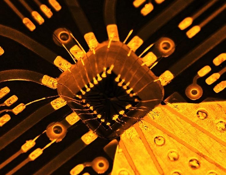
The silicon quantum computer chip used in this study. Photo credit: RIKEN Researchers from RIKEN and QuTech – a collaboration between TU Delft and TNO – have reached an important milestone in the development of a fault-tolerant quantum computer. They were able to demonstrate two-qubit gate accuracy of 99.5 percent — higher than the 99 percent considered the threshold for building fault-tolerant computers — using electron spin qubits in silicon, which show promise for large-scale quantum computing using nanofabrication technology their production already exists. The world is currently in a race to develop large quantum computers that could far outperform classical computers in certain areas. However, these efforts have been hampered by a number of factors, most notably the issue of decoherence, or the noise generated in the qubits. This problem becomes more severe with the number of qubits and hinders scaling. In order to achieve a large scale computer that could be used for useful applications, it is believed that a two-qubit gate accuracy of at least 99 percent is required to implement the surface code for error correction. This has been achieved in certain types of computers using qubits based on superconducting circuits, trapped ions, and nitrogen vacancy centers in diamond, but these are difficult to scale to the millions of qubits needed to implement practical quantum computations with an error correction. For the current work, published in Nature, the group decided to experiment with a quantum dot structure made by nanofabrication on a strained silicon/silicon-germanium quantum well substrate using a controlled NOT gate (CNOT). In previous experiments, the gate accuracy was limited due to the slow gate speed. To improve the gate speed, they carefully designed the device and tuned the device’s operating conditions by applying voltages to the gate electrodes to match the established fast single-spin rotation technique using micromagnets and a large two-qubit coupling combine. This allows them to increase the gate speed by a factor of 10 compared to the previous work. Interestingly, it used to be believed that increasing gate speed would always result in better fidelity, but they found that there was a limit and beyond that, increasing speed actually degraded fidelity. Through the work, they discovered that a property called the Rabi frequency — a marker for how the qubits change state in response to an oscillating field — is key to the system’s performance, and they found a range of frequencies for which the Single frequency qubit gate accuracy was 99.8 percent and two qubit gate accuracy was 99.5 percent, exceeding the required threshold. By doing so, they demonstrated that they can achieve universal operations, meaning that all fundamental operations that represent quantum operations, consisting of a single qubit operation and a two-qubit operation, can be performed with a gate accuracy above the error correction threshold. To test the performance of the new system, researchers implemented a two-qubit Deutsch-Jozsa algorithm and the Grover search algorithm. Both algorithms give correct results with a high accuracy of 96-97%, showing that silicon quantum computers can perform quantum calculations with high accuracy[{” attribute=””>accuracy. Akito Noiri, the first author of the study, says, “We are very happy to have achieved high-fidelity universal quantum gate set, one of the key challenges for silicon quantum computers.” Seigo Tarucha, leader of the research groups, said, “The presented result makes spin qubits, for the first time, competitive against superconducting circuits and ion traps in terms of universal quantum control performance. This study demonstrates that silicon quantum computers are promising candidates, along with superconductivity and ion traps, for research and development toward the realization of large-scale quantum computers. In the same issue of Nature, experimental demonstrations of similarly high-fidelity universal quantum gate sets achieved in silicon qubits are also reported from two independent research teams. A team at QuTech also used electron spin qubits in quantum dots (Quantum logic with spin qubits crossing the surface code threshold). Another team at UNSW Sydney (University of New South Wales) used a pair of ion-implanted phosphorous nuclei in silicon as nuclear spin qubits (Precision tomography of a three-qubit donor quantum processor in silicon). Reference: “Fast universal quantum gate above the fault-tolerance threshold in silicon” by Akito Noiri, Kenta Takeda, Takashi Nakajima, Takashi Kobayashi, Amir Sammak, Giordano Scappucci and Seigo Tarucha, 19 January 2022, Nature.DOI: 10.1038/s41586-021-04182-y See Major Breakthrough As Quantum Computing in Silicon Hits 99% Accuracy for more on this research.
Robot-Aided Assembly Could Speed Pace of Discovery for Incredible New Technologies
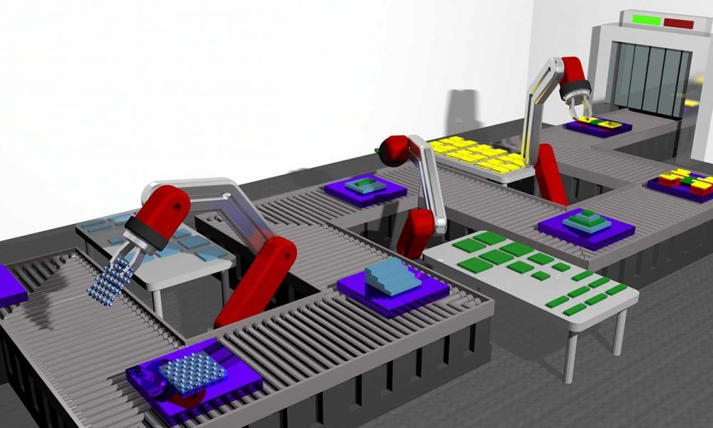
A breakthrough by University of Chicago scientists created a method to accelerate the search for potential new materials for electronics and other applications. Above is a conceptual representation of “robots” stacking thin films on an assembly line. Credit: Rendering by Andrew Ye Technology by UChicago scientists creates ‘assembly line’ for integration of new materials. Let’s say you are an engineer and you have an idea for a new car. But before you can even start experimenting, you’ll have to spend hours casting bolts and making rubber for tires from scratch. This is similar to the challenge researchers face when trying to invent new types of technology. The ability to make things like a flexible screen or a new solar panel starts with discovering a new combination of materials with unusual properties at the atomic level. But in the field of 2D materials, considered one of the most exciting areas for future electronics, scientists still have to painstakingly handcraft each new potential material before they can test its capabilities. A new technique asks a robot to help. Developed by scientists at[{” attribute=””>University of Chicago, Cornell University and the University of Michigan, the research lays out an innovative manufacturing method for assembling nanomaterials. The scientists hope the process, published recently in Nature Nanotechnology, could speed the pace of breakthroughs in the field. “This process is fully automated—you can program it and walk away,” said co-first author Andrew Mannix, a former University of Chicago Kadanoff-Rice postdoctoral fellow who is now an assistant professor at Stanford University. “Previously, if you wanted to try 10 different permutations of materials, it would all be done by hand, which is weeks of labor. We can now do this in an hour. We hope this opens new lines of inquiry in this exciting field by reducing the tediousness of labor.” A tiny assembly line The field of 2D materials involves stacking sheets that are each only a few atoms thick. When the layers are this thin, even ordinary materials often produce surprising new behaviors. For example, carbon suddenly displays superconductivity, the ability to conduct electricity flawlessly, when two layers are vertically stacked at a “magic” angle. “When we started looking at this problem, it seemed unimaginable to automate it.” — Prof. Jiwoong Park Scientists are especially interested in stacking together different kinds of 2D materials, Mannix said: “It’s been realized recently that if you can take these layers and stack them with control over the crystal orientation, you can get some really beautiful new physics, because the interactions between the layers are modified.” However, the discovery process is limited and slow, because scientists must first painstakingly assemble these combinations and test them one by one. UChicago scientists set out to address this problem. Led by Prof. Jiwoong Park, an expert on nanomaterials, the group had already invented a way to make intricate atomically-thin sheets and to peel them up and stack them together. Now they needed a way to automate this process. Scientists used the method to create a first-of-its-kind image of the atomic “texture” of a crystal assembled with four degrees of rotation between four layers. Credit: Image courtesy Mannix et al. They wanted to make a sort of tiny assembly line, but each component of the manufacturing process came with its own challenges. First, the scientists had to figure out a way to precisely cut their sheets into the exact shapes they wanted, which is difficult to do cleanly without breaking or damaging the sheets. “With experimentation, we found a technique that could achieve large-area patterning, with very high precision and without contaminating the material,” said Andrew Ye, a Ph.D. student in Park’s lab and the other co-first author of the paper. The next challenge was making a robot “hand” capable of maneuvering these extremely fragile sheets. “I needed to find a polymer that was precise enough to pick up the sheets,” said Mannix, “but also capable of letting it down again—gently and in the exact right spot.” They came up with a “hand” made of soft polymers that fall apart when exposed to heat or ultraviolet light. Once the sheet is precisely positioned, the hand dissolves and the sheet drops into place. With this system, the scientists could now program their assembly line to make a material structure with dozens of different layers, walk away, and come back to a finished sample ready to test in a matter of minutes. Not only is the system very precise, but it also offers extensive options for customization, including the coveted ability to rotate each successive sheet at different angles. “When we started looking at this problem, it seemed unimaginable to automate it,” said Park, who is appointed in both the Department of Chemistry and the Pritzker School of Molecular Engineering. “This should speed up the pace of discovery considerably. It’s kind of like the difference between handwriting a book letter by letter versus using a printing press.” Reference: “Robotic Four-Dimensional Pixel Assembly of van der Waals Solids” by Andrew J. Mannix, Andrew Ye, Suk Hyun Sung, Ariana Ray, Fauzia Mujid, Chibeom Park, Myungjae Lee, Jong-Hoon Kang, Robert Shreiner, Alexander A. High, David A. Muller, Robert Hovden and Jiwoong Park, 24 January 2022, Nature Nanotechnology.DOI: 10.1038/s41565-021-01061-5 The other authors on the study included University of Chicago graduate students Fauzia Mujid and Robert Shreiner; postdoctoral researchers Myungjae Lee and Jong-Hoon Kang; Chibeom Park, formerly a postdoctoral researcher and now at the Samsung Electronics Semiconductor Research Center; Prof. Alex High of the Pritzker School of Molecular Engineering and Argonne National Laboratory; Ariana Ray and Prof. David Muller of Cornell; and Suk Hyun Sung and Prof. Robert Hovden of the University of Michigan. The research made use of the University Chicago Materials Research Science and Engineering Center, the Pritzker Nanofabrication Facility, the Searle Cleanroom, the Michigan Center for Materials Characterization, and the Cornell Center for Materials Research. Funding: National Science Foundation, Air Force Office of Scientific Research, Samsung Advanced Institute of Technology, Department of Defense, W.M. Keck Foundation, Army Research

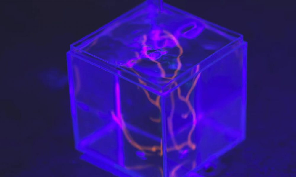
2D Material Identified That Can Store Quantum Information at Room Temperature
Artistic rendering of isolated spins on hexagonal boron nitride under a light microscope. Photo credit: Qiushi Gu Researchers have identified a two-dimensional material that could be used to store quantum information at room temperature. Quantum memory is a key building block that needs to be addressed in building a quantum internet, where quantum information is securely stored and sent via photons, or particles of light. “There are defects in this material that can emit single photons, which means it could be used in quantum systems.” — Hannah Stern Researchers at the University of Cambridge’s Cavendish Laboratory, in collaboration with colleagues from UT Sydney in Australia, have identified a two-dimensional material, hexagonal boron nitride, that can emit single photons at room temperature from atomic-scale defects in its structure. Researchers discovered that the light emitted by these isolated defects provides information about a quantum property that can be used to store quantum information, called spin, meaning the material could be useful for quantum applications. Importantly, the quantum spin is accessible via light and at room temperature. The finding could eventually support scalable quantum networks made of two-dimensional materials that can operate at room temperature. The results are published in the journal nature communication. Future communication networks will use single photons to send messages around the world, leading to more secure global communication technologies. Computers and networks based on the principles of quantum mechanics would be both far more powerful and safer than current technologies. However, to enable such networks, researchers need to develop reliable methods to generate single, indistinguishable photons as information carriers across quantum networks. “We can send information from one place to another using photons, but if we want to build real quantum networks, we need to send information, store it and send it somewhere else,” said Dr. Hannah Stern of the Cavendish Laboratory in Cambridge. Co-first author of the study, along with Qiushi Gu and Dr. John Jarman. “We need materials that can store quantum information for a period of time at room temperature, but most of the current material platforms that we have are difficult to fabricate and only work well at low temperatures.” Hexagonal boron nitride is a two-dimensional material grown by chemical vapor deposition in large reactors. It’s cheap and scalable. Recent efforts have revealed the existence of single photon emitters and the presence of a dense ensemble of optically accessible spin but not individually isolated spin-photon interfaces operating under ambient conditions. “Typically, it’s a pretty boring material that’s typically used as an insulator,” said Stern, a junior research fellow at Trinity College. “But we found that there are defects in this material that can emit single photons, which means it could be used in quantum systems. If we manage to store quantum information in the spin, then it’s a scalable platform.” Stern and her colleagues set up a hexagonal boron nitride sample near a tiny gold antenna and a fixed-strength magnet. By firing a laser at the sample at room temperature, they were able to observe many different magnetic-field-dependent responses to the light emitted by the material. The researchers found that by aiming the laser at the material, they were able to manipulate the spin, or inherent angular momentum, of the defects and use the defects as a way to store quantum information. “Usually the signal in these systems is always the same, but in this case the signal changes depending on the specific defect we’re investigating, and not all defects show a signal, so there’s still a lot to discover,” he said. First author Qiushi Gu. “There’s a lot of variation across the material, like a blanket draped over a moving surface – you see a lot of waves, and they’re all different.” Professor Mete Atature, who supervised the work, adds: “Having identified optically accessible isolated spins at room temperature in this material, the next steps will be to understand their photophysics in detail and the operational regimes for potential applications, including information storage and.” to investigate quantum sensors. After this work there will be a stream of fun physics.” Reference: “Magnetic Resonance Optically Captured at Room Temperature of Single Defects in Hexagonal Boron Nitride” by Hannah L. Stern, Qiushi Gu, John Jarman, Simone Eizagirre Barker, Noah Mendelson, Dipankar Chugh, Sam Schott, Hoe H. Tan, Henning Sirringhaus, and Igor Aharonovich Mete Atatüre, February 1, 2022, nature communication.DOI: 10.1038/s41467-022-28169-z The research was partially supported by the European Research Council. Mete Atature is a Fellow of St John’s College, Cambridge.